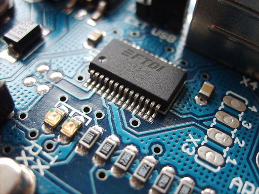
In the electronics industry’s product development, microanalysis and microscopy play a key role throughout the process. The analytical service XPS / ESCA instrument provided by Top Analytica Oy can measure the elemental distribution of semiconductor materials in the depth direction with a resolution of less than one nanometer. Ultra-thin coatings with ALD technology, for example, require accuracy that only XPS and ToF-SIMS are capable of.
The interfaces of the electronic components can only be examined by an electron microscope using only the ion cutter. With almost ten years of experience, we are able to produce samples with the goal required by pieteet.
As the latest acquaintance we have a RAMAN spectrophotometer. The relevant instrument can be used to view the silicon wafer flames from a large surface area.


